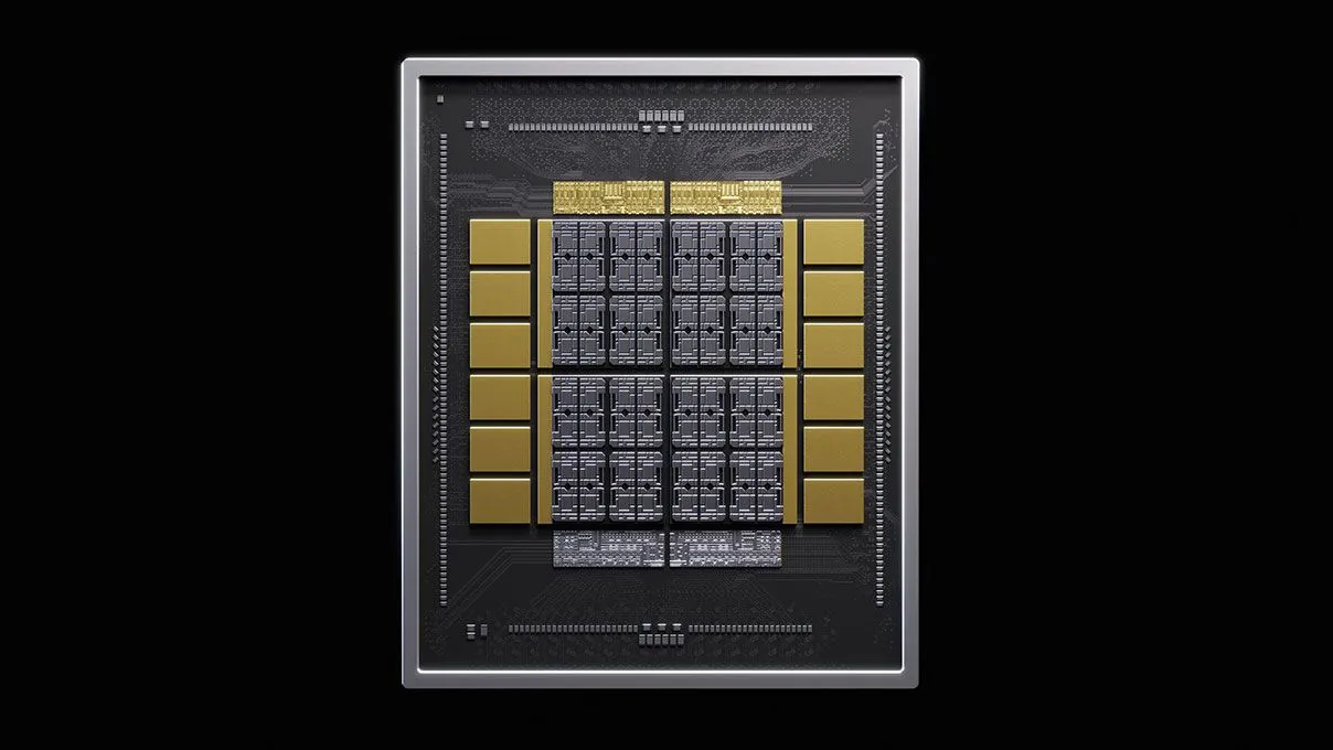
NVIDIA introduces NVHBM, a high-bandwidth memory with its controller built into the 3D stack. Result: up to 30% more bandwidth than HBM4E, with 15% lower power consumption and 25% more compute die area freed up.
A relocated memory controller for greater efficiency
Unlike traditional HBM, where the memory controller takes up space on the processor die (GPU, XPU, etc.), NVHBM integrates it into the base of the HBM stack itself. This approach, already planned for NVIDIA’s future GPUs, is now available to partners via NVLink Fusion. It frees up to 25% of the compute die area while improving performance.
Performance gains also come from a redesigned physical interface (PHY): NVIDIA claims to reduce the area occupied by I/Os by up to 67% compared to standard HBM4E, and simplify routing on the interposer, freeing up to 80% of usable layout area.
First partner: Amazon and its Trainium chips
Amazon, via its Annapurna Labs subsidiary, will be the first to adopt NVHBM as part of its collaboration with NVIDIA on NVLink Fusion. This technology will be integrated into future Trainium4 chips, enabling interoperability between Amazon processors and NVIDIA GPUs within a rack-scale architecture.
“NVHBM represents a new architectural approach to improve the performance and efficiency of high-bandwidth memory.” — Nafea Bshara, vice president of Annapurna Labs at AmazonTranslated from French
Standardization to accelerate adoption
NVIDIA offers a standardized implementation of NVHBM, available through multiple memory suppliers. The goal: reduce integration and qualification efforts for partners and speed up the market launch of semi-custom chips. NVLink Fusion, which connects custom XPUs to the NVIDIA ecosystem (NVLink chiplets, switches, MGX systems), complements this offering.
 RecommendedGeForce RTX 2080 Ti gets 22GB upgrade to rival $1000 AI GPUs
Context: memory shortages persist, factories multiply
Demand for memory, especially for AI, remains strong. SK hynix, one of the leading manufacturers, estimates that shortages will last until 2030 due to growing demand for custom DRAM and HBM configurations, which are less prone to oversupply. The company has also begun constructing a dedicated HBM assembly plant in the US, in West Lafayette (Indiana), at a cost of $4 billion. Volume production is expected in the second half of 2029.
This plant, which will employ 1,000 people, will focus on HBM assembly, testing, and R&D, using wafers produced in South Korea. SK hynix will also set up an advanced packaging R&D lab there, in partnership with Purdue University.
NVHBM fits into a broader trend: the vertical integration of memory components to meet the growing needs of AI. With concrete gains in bandwidth and energy efficiency, the technology could become a standard for semi-custom infrastructures, while players like SK hynix invest heavily to keep up with demand.
Sources
NVIDIA — NVIDIA NVLink Fusion Expands With NVHBM Custom High-Bandwidth Memory
TechPowerUp — NVIDIA NVHBM Memory Promises 30% Higher Bandwidth Than HBM4E
TechPowerUp — SK hynix CEO Says Memory Shortage Will Last Through 2030
Tom's Hardware — SK hynix breaks ground on the first HBM plant in the US




Comments 0
Sign in to join the discussion.
Be the first to comment.